Author: Dr Yu-Han Chang, Principal Technology Analyst at IDTechEx
Emerging advanced semiconductor packaging technologies, such as 2.5D and 3D hybrid bonding, are crucial for enhancing system performance across various applications such as AI and high-performance computing (HPC). This article explores the technology development trends in 2.5D and 3D packaging technologies and the key market growth drivers. The insights are derived from IDTechEx's recent report, “Advanced Semiconductor Packaging 2025-2035: Forecasts, Technologies, Applications“, which delves deep into understanding the technical aspects of packaging technologies, examining industry challenges, the progress made by leading companies, and providing market forecasts for the sector.
The evolution of semiconductor packaging technologies
Semiconductor packaging has evolved from traditional 1D PCB designs to cutting-edge 3D hybrid bonding at the wafer level. This advancement allows for interconnect pitches in the single-digit micrometer range and bandwidths up to 1000 GB/s, all while maintaining high energy efficiency. Central to advanced semiconductor packaging technologies are 2.5D packaging—where components are positioned side by side on an interposer—and 3D packaging, which involves stacking active dies vertically. These technologies are critical for the future of HPC systems.
2.5D packaging technologies involve various interposer materials, each offering distinct advantages and drawbacks. Silicon (Si) interposers, which include full passive Si wafers and localized Si bridges, are known for facilitating the finest routing features, making them ideal for high-performance computing. However, they come with high costs in both materials and manufacturing and face limitations in the packaging area. To mitigate these issues, the use of localized Si bridges is increasing, strategically utilizing silicon where fine features are essential and addressing area constraints.
Organic interposers, which use a fan-out molding compound, offer a more cost-effective alternative to silicon. They have a lower dielectric constant, which reduces RC delay in the package. Despite these benefits, organic interposers struggle to achieve the same level of interconnect feature reduction as silicon-based packages, limiting their adoption in high-performance computing applications.
Glass interposers have gained significant interest, particularly after Intel’s recent unveiling of a glass-based test vehicle package. Glass offers advantageous properties such as a tunable Coefficient of Thermal Expansion (CTE), high dimensional stability, a smooth as well as flat surface, and the ability to enable panel manufacturing, making it a promising candidate for interposers with routing features that could rival silicon. However, the main drawbacks of glass interposers are the immature ecosystem and the current lack of large-scale production capabilities, in addition to its technical challenges. As the ecosystem matures and production capabilities improve, glass-based technologies in semiconductor packaging may see further growth and adoption.
Regarding 3D packaging technologies, Cu-Cu bumpless hybrid bonding is emerging as a leading innovation. This advanced technique creates permanent interconnections by combining a dielectric material, such as SiO2, with embedded metal (Cu). Cu-Cu hybrid bonding can achieve pitches below 10 micrometers, typically in the single-digit micrometer range. This is a significant improvement over conventional microbump technology, which has a bump pitch of around 40-50 micrometers. The benefits of hybrid bonding include increased I/O, higher bandwidth, improved 3D vertical stacking, enhanced power efficiency, and reduced parasitics and thermal resistance due to the absence of underfill. However, this technique is complex to manufacture and comes with higher costs.

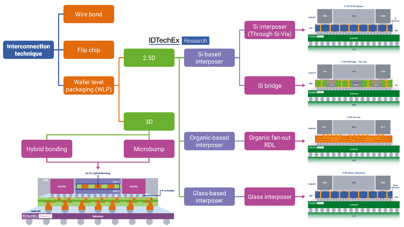
Overview of interconnection technique in semiconductor packaging. Source: IDTechEx – “Advanced Semiconductor Packaging 2025-2035: Forecasts, Technologies, Applications“
The 2.5D and 3D packaging technologies encompass various packaging techniques. In 2.5D packaging, the choice of interposer material categorizes it into Si-based, Organic-based, and glass-based interposers, as illustrated in the figure above. Meanwhile, in 3D packaging, the evolution of microbump technology aims for smaller pitch dimensions. However, achieving single-digit pitch dimensions today is made possible through the adoption of hybrid bonding technology. This method directly connects Cu-Cu, signifying a significant advancement in the field.
Key trends in 2.5D and 3D packaging development to watch
- Larger Interposer Areas
IDTechEx has previously predicted that 2.5D silicon bridge solutions will soon replace silicon interposers as the primary choice for packaging HPC chips due to the limitations of silicon interposers, which struggle to exceed 3x reticle sizes. TSMC, a key provider of 2.5D silicon interposers to NVIDIA and other major HPC developers like Google and Amazon, recently announced high-volume production of its first-generation CoWoS_L at 3.5x reticle size. IDTechEx expects this trend to continue, with further advancements explored in their report covering key players.
- Panel-Level Packaging
Panel-level packaging has become a significant focus, as highlighted at Semicon Taiwan 2024. This packaging method allows for larger interposers and helps reduce costs by enabling the production of more packages simultaneously. Despite its potential, challenges such as warpage management still need to be addressed. Its growing prominence reflects the increasing demand for larger and more cost-effective interposers.
- Glass Interposers
Glass is emerging as a strong candidate for enabling fine routing, comparable to silicon, with added benefits like tunable coefficient of thermal expansion (CTE) and improved reliability. Glass interposers are also compatible with panel-level packaging, offering the potential for high-density routing at a more manageable cost, making them a promising solution for future packaging technologies.
- Hybrid Bonding for HBMs
3D copper-copper (Cu-Cu) hybrid bonding is a critical technology for enabling ultra-fine pitch vertical interconnects between chips. This technology has already been used in several high-end server products, including AMD’s EPYC for stacking SRAM and CPUs, and the MI300 series for stacking CPU/GPU tiles on I/O tiles. Hybrid bonding is expected to play a pivotal role in future HBM advancements, particularly for DRAM stacks beyond 16-Hi or 20-Hi layers.
- Co-Packaged Optics (CPO)
Optical interconnect technology has gained considerable traction, driven by the growing need for higher data throughput alongside improved power efficiency. Co-packaged optics (CPO) is emerging as a key solution to enhance I/O bandwidth and reduce energy consumption. Optical communication offers multiple advantages over traditional electrical transmission, including lower signal degradation over distance, reduced susceptibility to crosstalk, and significantly higher bandwidth. These benefits make CPO an ideal fit for data-intensive, power-efficient HPC systems.
Key markets to watch
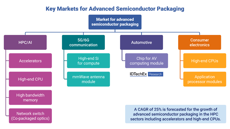
The primary market driving the development of 2.5D and 3D packaging technologies is undoubtedly the high-performance computing (HPC) sector. These advanced packaging methods are crucial in overcoming the limitations of Moore's law, enabling more transistors, memory, and interconnections within a single package. The disaggregation of chips also allows for optimal process node utilization across different functional blocks, such as separating I/O tiles from processing tiles, further enhancing efficiency.
Beyond HPC, other markets are poised for growth through the adoption of advanced packaging technologies. In the 5G and 6G sectors, innovations like antenna-in-package and cutting-edge chip solutions will shape the future of radio access network (RAN) architectures. Autonomous vehicles will also benefit, as these technologies support the integration of sensor suites and computing units to process large volumes of data while ensuring safety, reliability, compactness, power and thermal management, and cost-effectiveness.
Consumer electronics—including smartphones, smartwatches, AR/VR devices, PCs, and workstations—though more cost-conscious, are increasingly focused on handling more data within smaller spaces. Advanced semiconductor packaging will play a key role in this trend, though the packaging methods will differ from those used in HPC. IDTechEx provides in-depth analysis of these industries, examining how advanced packaging technologies will impact them and offering market forecasts.

Key markets for advanced semiconductor packaging. Source: IDTechEx – “Advanced Semiconductor Packaging 2025-2035: Forecasts, Technologies, Applications“
What is in the newly released IDTechEx report?
The new IDTechEx report, “Advanced Semiconductor Packaging 2025-2035: Forecasts, Technologies, Applications”, thoroughly explores the latest innovations in semiconductor packaging technology, covering key technical trends, analyzing the value chain, evaluating major players, and providing detailed market forecasts.
Recognizing the crucial role of advanced semiconductor packaging as the foundation for next-generation ICs, the report focuses on its applications in key markets such as AI and data centers, 5G, autonomous vehicles, and consumer electronics. Leveraging IDTechEx's expertise in these sectors, the report delivers a comprehensive understanding of the impact and future trajectory of advanced semiconductor packaging in these critical fields.
Key aspects of this report:
Exploring technology trends and manufacturers in advanced semiconductor packaging:
- Explore advanced semiconductor packaging evolution, addressing transistor IC challenges. Examine how chiplet concepts and heterogeneous integration propel advanced packaging adoption.
- Analyze Packaging Technologies: Segment by interposer material (Si, Glass, Organic), covering roadmaps, benchmarks, applications, players, and manufacturing barriers.
- Company Analysis: In-depth examination of key companies, assessing solutions, clientele, applications, and technology roadmap.
- Key Markets: Provide detailed overviews for critical markets – high-performance computing, autonomous vehicles, 5G, and consumer electronics.
- Case Studies: Showcase various industry applications of advanced semiconductor packaging.
- Supply Chain & Models: Analyze supply chain dynamics and business models in this evolving landscape.
10-year granular market forecasts and analysis:
- Data Center Server Unit Forecast 2023-2035 (Shipment)
- Data Center CPU: Advanced Semiconductor Packaging Forecast 2023-2035 (Shipment)
- Data Center Accelerator: Semiconductor Packaging Forecast 2023-2035 (Shipment)
- 2.5D Semiconductor Packaging for L4+ Autonomous Vehicles 2023-2045
- 3D Semiconductor Packaging for L4+ Autonomous Vehicles 2023-2045
- Consumer Electronics Unit Sales Forecast 2023-2035 (Smartphones/Tablets/Smartwatches/AR/VR/MR)
- Advanced Semiconductor Packaging Forecast for APE in Consumer Electronics 2023-2035
- Global PC Shipment Forecast 2023-2035
- Advanced Semiconductor Packaging in PC Forecast 2023-2035
- 5G Radios by MIMO Size Unit Forecast 2023-2035
- Advanced Semiconductor Packaging for 5G RAN Networks 2023-2035
- Total CPO market forecast in revenue 2023-2035
To find out more about this new IDTechEx report, including downloadable sample pages, please visit www.IDTechEx.com/ASP.
For the full portfolio of semiconductor market research available from IDTechEx, please see www.IDTechEx.com/Research/Semiconductors.


